<?xml version="1.0" encoding="utf-8"?><feed xmlns="http://www.w3.org/2005/Atom" ><generator uri="https://jekyllrb.com/" version="3.10.0">Jekyll</generator><link href="https://filippomoro.github.io/feed.xml" rel="self" type="application/atom+xml" /><link href="https://filippomoro.github.io/" rel="alternate" type="text/html" /><updated>2026-09-04T21:55:37+00:00</updated><id>https://filippomoro.github.io/feed.xml</id><title type="html">About me</title><subtitle>Filippo&apos;s personal webpage</subtitle><author><name>Filippo Moro</name><email>filippo.moro@uzh.ch</email></author><entry><title type="html">Three Levels of Biological Inspiration: Bridging NeuroAI and Neuromorphic Engineering</title><link href="https://filippomoro.github.io/talks/2026-03-17-Cosyne2026_NeuroAI" rel="alternate" type="text/html" title="Three Levels of Biological Inspiration: Bridging NeuroAI and Neuromorphic Engineering" /><published>2026-03-21T00:00:00+00:00</published><updated>2026-03-21T00:00:00+00:00</updated><id>https://filippomoro.github.io/talks/cosyne2026_neuroai</id><content type="html" xml:base="https://filippomoro.github.io/talks/2026-03-17-Cosyne2026_NeuroAI"><![CDATA[<p>Artificial Intelligence is advancing at ever increasing speed, learning from massive data and running in huge datacenters. Modern AI does not look much like biological intelligence. So what role does neuroscience play in the context of AI? This question was at the center of a recent workshop organized at Cosyne 2026: “Biologically-Inspired Artificial Intelligence”. Here I show my perspective on this intriguing research question, structuring inspiration from biology into three distinct levels: mechanical, system-level, and behavioral. As a neuromorphic engineer, I am used to working at the mechanical level, replicating the biophysics of neurons and synapses with electronics. However, I see great opportunities to work at a higher level of abstraction by drawing inspiration from biological computation. This hints at the unification of NeuroAI with Neuromorphic Computing.</p>

<hr />

<p>I had the fantastic opportunity to speak at <a href="https://www.cosyne.org/">Cosyne 2026</a>, in the workshop on <a href="https://sites.google.com/view/cosyne-neuroai/"><em>Biologically-Inspired Artificial Intelligence</em></a>. Cosyne is one of the leading conferences in (computational) neuroscience, and it was my first time attending it. The community is creative, welcoming, and genuinely curious about the deep questions at the intersection of biology and computation. Being an engineer surrounded by computational neuroscientists for a few days was truly inspiring.</p>

<h1 id="what-role-does-neuroscience-play-in-the-age-of-ai">What Role Does Neuroscience Play in the Age of AI?</h1>

<p>It is hard to ignore that AI is advancing at a pace that would have seemed implausible just a few years ago. Large language models are reshaping the concept of intelligence and, notably, do not look much like brains. Backpropagation through deep networks, attention mechanisms, and massive parallelism on GPU clusters are a long way from local plasticity, spike-timing-dependent learning, and the roughly 20 watts of power consumed by the human brain.</p>

<p>So <em>what role does neuroscience play in this context?</em> Is biological inspiration still a useful guide for building intelligent systems, or has it become more of an aesthetic preference?</p>

<p>As a neuromorphic engineer, I feel this growing <strong>tension</strong>. Neuromorphic computing has historically drawn deep inspiration from biology, often at the level of mimicking individual neurons and synapses. But as the gap between neuromorphic hardware and state-of-the-art AI grows wider, it becomes worth asking: <em>are we drawing the right kind of inspiration?</em></p>

<h1 id="three-levels-of-biological-inspiration">Three Levels of Biological Inspiration</h1>

<p>I find it useful to distinguish between three levels, which map onto different parts of the stack of engineering intelligence — from devices and circuits all the way up to applications and algorithms.</p>

<p align="center">
  <img src="/images/Blog_Cosyne2026/Three_Level_BioInspiration.jpg" width="70%" alt="Three levels of biological inspiration: mechanical, system, and behavioral" />
</p>
<p align="center">
  <em>Courtesy of Melika Payvand.</em>
</p>

<h2 id="1-mechanical-level">1. Mechanical Level</h2>

<p>The mechanical level is about faithfully <strong>mimicking the biophysics of neural computation</strong>: the dynamics of individual neurons, synapses, axons, and dendrites. This is where traditional neuromorphic engineering has lived, designing circuits that reproduce the biophysical dynamics of real neurons, memristive devices that implement synaptic plasticity, or architectures that implement dendritic compartments.</p>

<p>The mechanical level asks: <em>what of the complex neuronal biophysics is useful for computation and how?</em></p>

<h2 id="2-system-level">2. System Level</h2>

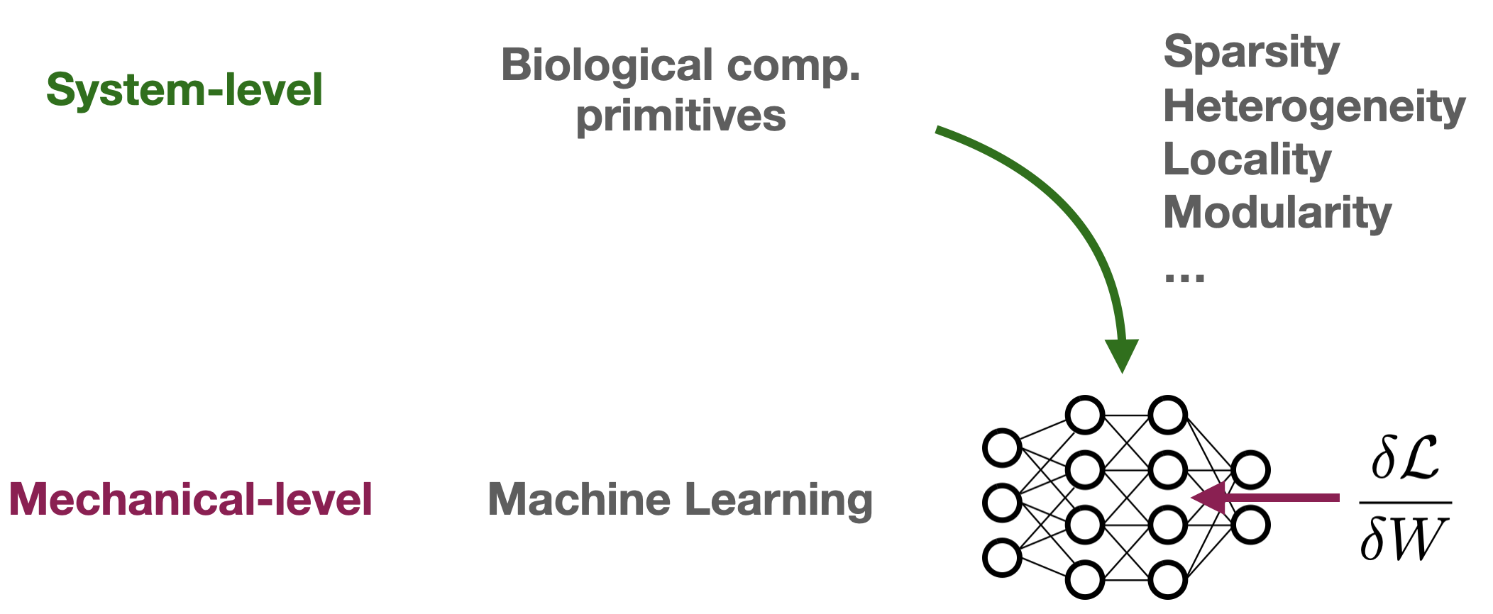
<p>The system level takes a step up, adopting the “mechanisms” of machine learning — artificial neural networks and backpropagation — but inject biological <em>system-level</em> features: heterogeneity across neurons, functional specialization of different brain areas, sparse connectivity, modularity, or principles like neurogenesis. It’s not trying to replicate the biophysics, it’s rather making the hypothesis that the <em>organisational principles</em> of biological neural systems can make artificial ones better.</p>

<p>The system level asks: <em>can biological organizational principles improve the function of artificial networks?</em></p>

<h2 id="3-behavioral-level">3. Behavioral Level</h2>

<p>The behavioral level draws inspiration from how brains <em>act</em>, rather than how they are built. This is closest to classical AI: designing systems that exhibit intelligent behaviors such as perception, decision-making, and creativity, observed in animals, without necessarily caring about the underlying substrate.</p>

<p>Notably, this level is as much about sensing as it is about computation: behavior, after all, emerges from the interaction with an environment. This makes behavioral inspiration particularly relevant for embodied AI, though not exclusively: systems like large language models draw on behavioral inspiration while operating purely in the symbolic domain.</p>

<h2 id="where-neuromorphic-and-neuroai-currently-live">Where Neuromorphic and NeuroAI Currently Live</h2>

<p>Neuromorphic engineering has traditionally operated at the <strong>mechanical level</strong>, while NeuroAI has worked mainly between the <strong>system</strong> and <strong>behavioral</strong> levels. But I believe both fields have much to gain from moving across this hierarchy, forming a synergy.</p>

<p>This is also the direction my lab — the <a href="https://esl.epfl.ch/research/the-eis-lab/">Emergent Intelligent Substrates (EIS) Lab</a>, led by Prof. Melika Payvand — has been pursuing.</p>

<h1 id="what-we-work-on">What We Work On</h1>

<p>Let me show you what this looks like in practice across two of these levels.</p>

<h2 id="mechanical-level-dendritic-delays">Mechanical Level: Dendritic Delays</h2>

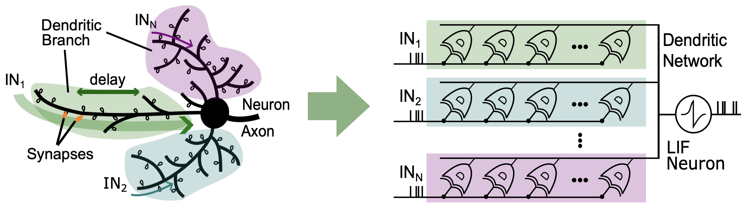
<p>Dendrites exhibit a rich repertoire of computational primitives, one of which is the <strong>propagation delay</strong> of pre-synaptic stimuli as they travel toward the soma. This delay is a form of temporal memory built directly into the morphology of the neuron.</p>

<p align="center">
  <img src="/images/Blog_Cosyne2026/DenRAM.png" width="90%" alt="DenRAM - Dendritic architecture with delays" />
</p>
<p align="center">
  <em>DenRAM mimics dendritic arbors with synaptic elements that delay and weigh input spikes, converging to an output Leaky-Integrate-and-Fire neuron.</em>
</p>

<p>In <strong>DenRAM</strong> (<a href="https://www.nature.com/articles/s41467-024-57108-x">D’Agostino, Moro et al., <em>Nature Communications</em> 2024</a>), we built a neuromorphic hardware architecture that uses Resistive RAM (RRAM) to implement dendritic delays with ultra-low power consumption. Delay-based spiking networks turn out to be significantly more efficient than recurrent models: we demonstrated a <strong>5× reduction in power</strong> and up to a <strong>35× reduction in memory footprint</strong> on ECG anomaly detection and keyword spotting benchmarks.</p>

<p>One limitation of DenRAM is that it does not train the delays explicitly. This motivated <strong>DelGrad</strong> (<a href="https://www.nature.com/articles/s41467-025-57628-w">Göltz, Weber, Kriener et al., <em>Nature Communications</em> 2025</a>), an algorithm that derives exact, event-based gradients for both synaptic weights <em>and</em> delays in spiking networks. DelGrad is compatible with LIF neurons and has been validated on neuromorphic hardware (BrainScaleS), where training axonal delays reduces test error meaningfully even under the noise of analog hardware.</p>

<p>Together, DenRAM and DelGrad make the case that the mechanical richness of dendrites — specifically, their temporal structure — is a powerful computational resource.</p>

<h2 id="system-level-heterogeneous-memory-temporal-hierarchy-and-neurogenesis">System Level: Heterogeneous Memory, Temporal Hierarchy, and Neurogenesis</h2>

<p>Moving up the hierarchy, we have been working on how biological system-level principles can improve artificial networks trained with backpropagation.</p>

<p align="center">
  <img src="/images/Blog_Cosyne2026/System_level.png" width="90%" alt="System-level of biological inspiration" />
</p>
<p align="center">
  <em>In the system-level of biological inspiration, we leverage machine-learning computational mechanisms in conjunction with high-level features of biological computations.</em>
</p>

<p><strong>mGRADE</strong> (<a href="https://arxiv.org/abs/2507.01829">Torchet et al., <em>arXiv</em> 2025</a>) combines two ideas: the minimal gated recurrent unit (minGRU) for processing slow temporal dynamics, and dilated convolutions with learnable spacings (DCLS) for capturing fast temporal features. The result is a deep recurrent network with <strong>heterogeneous memory</strong> — inspired by the fact that brains exhibit heterogeneous strategies for memory formation. mGRADE achieves state-of-the-art performance on the Long Range Arena benchmark and on raw-audio keyword spotting, while being the only architecture in its class small enough to fit on common microcontrollers.</p>

<p><strong>Temporal Hierarchy in SNNs</strong> (<a href="https://arxiv.org/abs/2407.18838">Moro et al., <em>arXiv</em> 2024</a>) investigates whether the hierarchy of intrinsic timescales observed in the mammalian cortex — where deeper cortical areas process information over longer timescales — is also useful as an inductive bias in artificial spiking networks. The answer is yes: imposing a structured gradient of time constants across hidden layers consistently improves performance on temporal tasks, and interestingly, this hierarchy <em>also emerges spontaneously from optimization</em> when networks are trained on sequential data.</p>

<p><strong>GroHess</strong> takes inspiration from adult hippocampal neurogenesis — the brain’s ability to grow new neurons as a mechanism for continual learning — and implements a biologically-motivated artificial counterpart. Using information-geometry-based triggers (effective dimensionality and Fisher saturation metrics), the algorithm decides <em>when</em> and <em>where</em> to grow new neurons, and initialises them orthogonally to the existing representations to minimise interference. On both Split MNIST and Permuted MNIST, GroHess achieves better performance with smaller final models than static baselines.</p>

<h1 id="looking-ahead-a-synergy-worth-pursuing">Looking Ahead: A Synergy Worth Pursuing</h1>

<p>I believe the future of both fields lies in their convergence.</p>

<p><strong>NeuroAI</strong> would benefit from engaging more seriously with neuromorphic hardware. Energy-efficient substrates impose structure that may turn out to be a feature rather than a limitation: sparse connectivity, modular networks and local learning rules are all biologically motivated and increasingly attractive from an engineering standpoint.</p>

<p><strong>Neuromorphic engineering</strong> should break free from its focus on the mechanical level. The most impactful near-term opportunities may lie in the system level: using the organizational principles of biological brains — hierarchy of time-scales, heterogeneous dynamics, modular connectivity — to build systems that are simultaneously more efficient and more functional.</p>

<p>The next step is to build systems that are neuromorphic in substrate, biologically-organized at the system-level, while leveraging the powerful computational tools of machine learning. I think we are closer to that than it might seem.</p>

<hr />

<p><em>Filippo Moro is a Postdoc in the <a href="https://esl.epfl.ch/research/the-eis-lab/">EIS Lab</a> at UZH and ETH Zurich, led by Prof. Melika Payvand. His research sits at the intersection of neuromorphic hardware, spiking neural networks, and biologically-inspired machine learning.</em></p>]]></content><author><name>Filippo Moro</name><email>filippo.moro@uzh.ch</email></author><category term="neuromorphic" /><category term="neuroai" /><category term="cosyne" /><category term="spiking-neural-networks" /><category term="biological-inspiration" /><summary type="html"><![CDATA[Artificial Intelligence is advancing at ever increasing speed, learning from massive data and running in huge datacenters. Modern AI does not look much like biological intelligence. So what role does neuroscience play in the context of AI? This question was at the center of a recent workshop organized at Cosyne 2026: “Biologically-Inspired Artificial Intelligence”. Here I show my perspective on this intriguing research question, structuring inspiration from biology into three distinct levels: mechanical, system-level, and behavioral. As a neuromorphic engineer, I am used to working at the mechanical level, replicating the biophysics of neurons and synapses with electronics. However, I see great opportunities to work at a higher level of abstraction by drawing inspiration from biological computation. This hints at the unification of NeuroAI with Neuromorphic Computing.]]></summary></entry><entry><title type="html">The Memory Technology Landscape</title><link href="https://filippomoro.github.io/posts/2024/11/The%20Memory%20Technology%20Landscape/" rel="alternate" type="text/html" title="The Memory Technology Landscape" /><published>2024-11-14T00:00:00+00:00</published><updated>2024-11-14T00:00:00+00:00</updated><id>https://filippomoro.github.io/posts/2024/11/The-Memory-Technology-Landscape%20copy</id><content type="html" xml:base="https://filippomoro.github.io/posts/2024/11/The%20Memory%20Technology%20Landscape/"><![CDATA[<p>Memory technology has become the major battleground for integrated chip innovation. Our chips’ integrated memory is ever-growing and now occupies a considerable portion of commercial silicon dies. While Static-Random-Access-Memory technology dominates the on-chip memory market, a recent <a href="https://en.eeworld.com.cn/mp/Icbank/a155559.jspx">article</a> pointed out that SRAM’s scaling - fueled so far by Moore’s Law - is hitting a wall. TSMC’s 3nm node only provides a minor 5% improvement in SRAM bitcell density compared to the 5nm node. So what is the future for on-chip memory?</p>

<p>Here I explore the current on-chip memory landscape to extrapolate what the future might look like. More importantly, this article links to a <a href="https://docs.google.com/spreadsheets/d/1qB0eTERsOAq3VRLizeE9IMj2wXXSUNgyxcXAxigXpuM/edit?gid=0#gid=0">spreadsheet</a> where I gather data on all the memory devices featured in the plots. You can access this spreadsheet freely and will find all the information about the given memory devices, as well as a reference to the scientific paper in which they were featured.</p>

<h1 id="memory-is-all-you-need">Memory is all you need</h1>
<p>Memory technology has become the major battleground for integrated chip innovation. Our chips’ integrated memory is ever-growing and now occupies a considerable portion of commercial silicon dies. While Static-Random-Access-Memory technology dominates the on-chip memory market, an article pointed out that SRAM’s scaling - fueled so far by Moore’s Law - is hitting a wall [1]. TSMC’s 3nm node only provides a minor improvement (about 5%) in SRAM bitcell density compared to the 5nm node. So what is the future for on-chip memory?</p>

<p>Some suggest that the shift from FinFET to Nanosheet transistor technology will propel the continuation of CMOS - and SRAM as well - scaling. Others highlight that alternative solutions exist: several emerging memory cells have been developed with the aim of going beyond standard CMOS and exploiting different physical phenomena to store information in memory cells. Among such innovative devices are Resistive-RAM (RRAMs) [2], Phase-Change-Memory (PCM) [3], Magnetic-RAM (MRAM) [4], Ferroelectric-RAM (FeRAM) [5], 2T-Gain-Cells [6], and eDRAM [7]. Although far less mature than SRAM, these devices (except for 2T-Gain-Cells and eDRAM) are non-volatile, thus promising energy efficiency, and can easily be integrated into the Back-End-of-Line (BEOL) of common CMOS processes, enabling high memory integration density.</p>

<p>This article offers a bird’s-eye view of the memory technology landscape, analyzing SRAM development down to the most recent nodes and assessing the performance of alternative emerging memory devices. Importantly, this article is inspired by this excellent review <a href="https://ieeexplore.ieee.org/abstract/document/10488872">paper</a> from Prof. Shimeng Yu. I build on top of this article by finding relevant sources in the literature and providing my own opinions on the future of memory technology. You can access all the information contained in this article from this <a href="https://docs.google.com/spreadsheets/d/1qB0eTERsOAq3VRLizeE9IMj2wXXSUNgyxcXAxigXpuM/edit?gid=0#gid=0">spreadsheet</a>: it features scientific references and technical information on many memory devices.</p>

<h2 id="sram-scaling">SRAM scaling</h2>
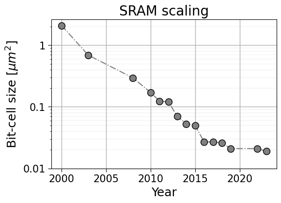
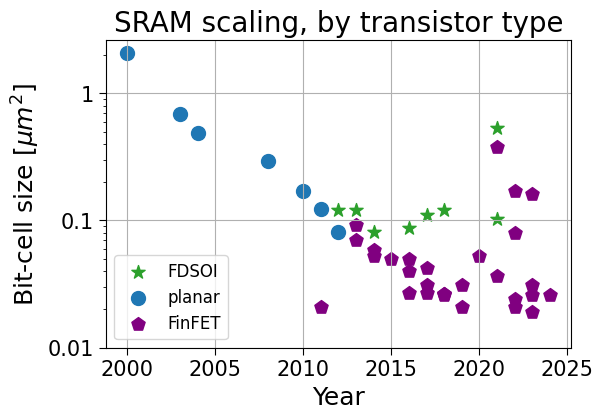
<p>Pushed by advances in transistor technology, SRAM performance has improved at an astounding pace over the years. Here we focus on SRAM scaling after the year 2000, showing the impressive rate at which cell size has shrunk.</p>

<!-- <p align="center">
  <img src="/images/Blog_Memory/SRAM_scaling.png" alt="alt text" width="1200"/>
</p> -->

<style>
  .figure-carousel {
    position: relative;
    max-width: 900px;
    margin: 1rem auto 2rem;
  }

  .carousel-track {
    position: relative;
    width: 100%;
  }

  .carousel-slide {
    display: none;
    width: 85%;
    height: auto;
  }

  .carousel-slide.is-active {
    display: block;
  }

  .carousel-btn {
    position: absolute;
    top: 50%;
    transform: translateY(-50%);
    z-index: 2;
    border: 0;
    background: rgba(0, 0, 0, 0.55);
    color: #fff;
    font-size: 1.5rem;
    line-height: 1;
    padding: 0.5rem 0.75rem;
    cursor: pointer;
  }

  .carousel-btn.prev {
    left: 0.5rem;
  }

  .carousel-btn.next {
    right: 0.5rem;
  }

  .carousel-btn:focus-visible {
    outline: 2px solid #ffffff;
    outline-offset: 2px;
  }
</style>

<p>Scroll through the 3 figures!</p>
<div class="figure-carousel" data-carousel="">
  <button class="carousel-btn prev" type="button" aria-label="Previous figure">‹</button>
  <div class="carousel-track">
    <img class="carousel-slide is-active" src="/images/Blog_Memory/SRAM_scaling_general.png" alt="SRAM scaling - general" />
    <img class="carousel-slide" src="/images/Blog_Memory/SRAM_scaling_company.png" alt="SRAM scaling - by company" />
    <img class="carousel-slide" src="/images/Blog_Memory/SRAM_scaling_transistor.png" alt="SRAM scaling - by transistor architecture" />
  </div>
  <button class="carousel-btn next" type="button" aria-label="Next figure">›</button>
</div>

<script>
  document.addEventListener("DOMContentLoaded", function () {
    document.querySelectorAll("[data-carousel]").forEach(function (carousel) {
      const slides = Array.from(carousel.querySelectorAll(".carousel-slide"));
      const prev = carousel.querySelector(".prev");
      const next = carousel.querySelector(".next");
      let index = slides.findIndex(function (slide) {
        return slide.classList.contains("is-active");
      });

      if (index < 0) {
        index = 0;
      }

      function render() {
        slides.forEach(function (slide, i) {
          slide.classList.toggle("is-active", i === index);
        });
      }

      prev.addEventListener("click", function () {
        index = (index - 1 + slides.length) % slides.length;
        render();
      });

      next.addEventListener("click", function () {
        index = (index + 1) % slides.length;
        render();
      });

      render();
    });
  });
</script>

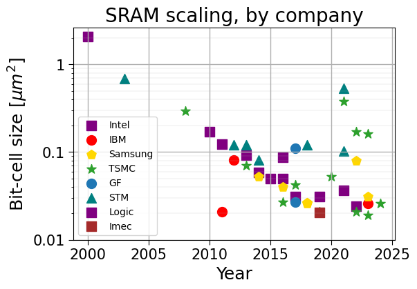
<p>This data, again, is reported in the shared <a href="https://docs.google.com/spreadsheets/d/1qB0eTERsOAq3VRLizeE9IMj2wXXSUNgyxcXAxigXpuM/edit?gid=0#gid=0">spreadsheet</a> and from it we can learn three main messages:</p>
<ul>
  <li>1: SRAM bit-cell size has steadily decreased through the years, but it appears to have slowed down lately.</li>
  <li>2: planar CMOS technology hit a wall at the beginning of the 2010s, when FinFET technology took over and continued the scaling trend.</li>
  <li>3: only three companies are currently participating in the race of SRAM scaling (TSMC, Samsung, Intel).</li>
</ul>

<!-- It's important to note that in the early 2010's, performance of bulk CMOS was stagnating due to the limited electrostatic control over the channel. The semicoductor industry was quick to react and adopt a novel transistor architecture, the FinFET transitor, capable of a greater control over the channel and thus enable further scaling of feature sizes. More recently, it seems the FinFET has reached its limitations and SRAM size has slowed down. However, the industry has prepared an evolution of the FinFET transistor, the Nano-sheet-FET, which should drive the innovation of CMOS tecnology - and SRAM as well - in the coming years. -->
<p>As technology nodes become more advanced, the investments required to participate in the silicon scaling race grow exponentially. This is why the leading edge of SRAM scaling is carried out by essentially only one company nowadays, TSMC. Samsung follows closely, and Intel seems to be lagging a little behind.</p>

<h2 id="will-sram-scaling-continue">Will SRAM scaling continue?</h2>

<p>It seems like SRAM scaling is becoming harder and harder, and even TSMC flinched when launching its 3nm node, with the N3B specification offering only a 5% improvement over the N5 (5nm) node [1].
However, the semiconductor industry still has some tricks up its sleeves, and it is ready to play them all to ensure the continuation of SRAM scaling.</p>
<ul>
  <li><strong>Nanosheet transistors</strong>: the next generation of transistors promises higher integration density, guaranteeing the continuation of SRAM scaling.</li>
  <li><strong><a href="https://www.intel.com/content/www/us/en/newsroom/news/powervia-test-shows-industry-leading-performance.html">Backside power rails</a></strong>: an option mainly researched by Intel.</li>
  <li><strong><a href="https://spectrum.ieee.org/forksheet-transistor">Forksheet transistor</a></strong>: a development of Gate-All-Around transistors enabling greater transistor density.</li>
  <li><strong><a href="https://www.allaboutcircuits.com/news/from-finfets-to-cfets-imecs-plan-for-continued-transistor-scaling/">Complementary 3D stacked logics</a></strong>: a potentially disruptive technology whereby p- and n-mos transistors can be stacked on top of each other, offering clear scaling advantages even compared to ultimate nanosheet transistors.</li>
</ul>

<h1 id="alternative-emerging-memory-technology">Alternative emerging memory technology</h1>

<h2 id="embedded-non-volatile-memory-envm">Embedded Non-Volatile Memory (eNVM)</h2>
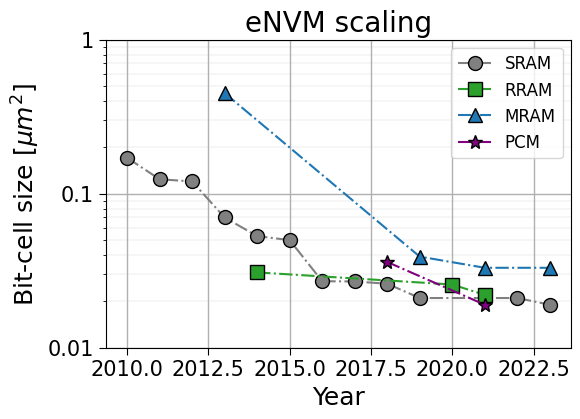
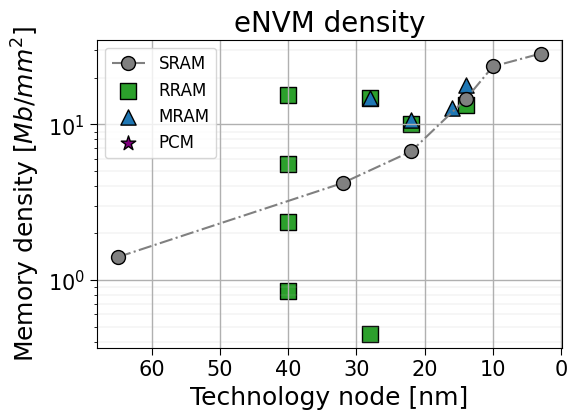
<p>As advanced technology nodes become ever more expensive and technically challenging, very few companies can afford to continue CMOS development. This leads researchers to explore novel memory devices that operate by exploiting different physical phenomena. This class of emerging memories has been discussed a lot, so how does it compare with SRAM? We’ll now focus on emerging non-volatile memory (eNVM), which includes RRAM, MRAM, PCM, and FeRAM. (The latter is not mature enough to be compared in the following plots.)</p>

<p>Scroll through the 2 figures!</p>
<div class="figure-carousel" data-carousel="">
  <button class="carousel-btn prev" type="button" aria-label="Previous figure">‹</button>
  <div class="carousel-track">
    <img class="carousel-slide is-active" src="/images/Blog_Memory/eNVM_scaling_general.png" alt="eNVM scaling overview" />
    <img class="carousel-slide" src="/images/Blog_Memory/eNVM_density_general.png" alt="eNVM memory density overview" />
  </div>
  <button class="carousel-btn next" type="button" aria-label="Next figure">›</button>
</div>

<p>This data, once more, is reported in the shared <a href="https://docs.google.com/spreadsheets/d/1qB0eTERsOAq3VRLizeE9IMj2wXXSUNgyxcXAxigXpuM/edit?gid=0#gid=0">spreadsheet</a>:</p>
<ul>
  <li>1: in terms of bit-cell size, eNVM is competitive with SRAM, especially RRAM and PCM.</li>
  <li>2: however, memory array density highlights that eNVM is, for now, reserved for larger technology nodes (typically 40nm or 28nm, topping at 14nm), and thus eNVM is currently less memory-dense.</li>
</ul>

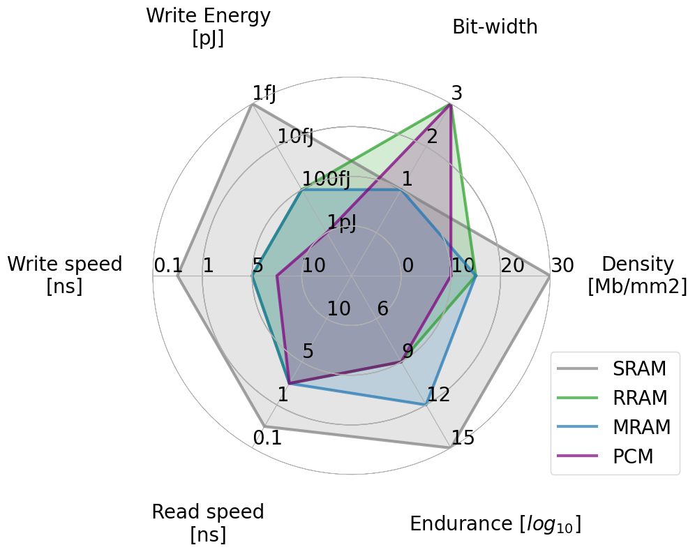
<p>For now we have mainly looked at size and density, but there is more to memory. The next figure gives an idea of the figures of merit of different memory technologies, comparing SRAM (in gray) to eNVM. Note that this figure is obtained by considering the general performance of the different memory classes, taking inspiration from Table 1 in [8].</p>

<p><img src="/images/Blog_Memory/Memory_overview.png" alt="alt text" width="550" /></p>

<p>What do we learn? SRAM and eNVM are apples and oranges. They do not belong to the same class of memory devices, which are famously clustered in the memory pyramid (refer to Figure 2 in [8]). In particular, the core differences are:</p>
<ul>
  <li>SRAM is <em>fast</em>! eNVM is slower to read and even slower to write.</li>
  <li>SRAM has extremely high endurance (number of read/write cycles before failure). MRAM also features high endurance, but RRAM and PCM are very limited in this sense.</li>
  <li>Despite SRAM being the densest so far, RRAM and PCM feature multi-bit per cell. The density gap might close in the future!</li>
</ul>

<!-- #### Gain Cell (eDRAM) and embedded Flash -->

<h1 id="the-future-of-memory-technology">The future of memory technology</h1>

<!-- SRAM is still too good, will stay there for cache L1 and L2 for sure
MRAM as alternative for L3/4
CIM is the battleground for eNVM -> memory density is key, going 3D [9] is the way to truly innovate! -->
<p>(What follows is my personal opinion)</p>

<p>It is hard to predict what the future of memory technology will look like. My opinion is that until transistor scaling will be physically possible and economically viable, industry will keep developing in that direction, bringing benefits to SRAM scaling. Concerning memory applications, it’s hard to see SRAM dethroned as L1 and L2 cache memory, where sheer speed is mandatory. There is no other device currently capable to deliver similar read and write speed.</p>

<p>However, transistor scaling will likely hit a point of diminishing returns at some point. Are the alternative memory devices ready to take over when this happens? Again, it depends on the applications.</p>
<ul>
  <li>eNVM is <em>already</em> in the market, as embedded memory in commercial micro-controllers [9].</li>
  <li>As L3 or L4 cache memory, MRAM might evolve into a serious candidate, especially when its non-volatility can be exploited in low stand-by power contexts.</li>
</ul>

<h2 id="compute-in-memory">Compute-In-Memory</h2>
<p>The most intriguing domain of application for eNVM is certainly Compute-in-Memory (CIM). While SRAM-based CIM is definitely high-performing, breaking the 1000 Tops/W mark per macro, eNVM-based CIM is also competitive [10]. eNVM features two important characteristics that are still not fully exploited in CIM, especially in low-power applications. While SRAM is the speed king and maximally efficient only at peak frequency, eNVM does not consume any static power (in theory!), and it is thus energy-efficient even at low frequency, a typical use case for edge applications. Also, RRAM and PCM store multiple bits per cell (typically 3 bits): this aspect is rarely exploited as it makes peripheral circuit design more complex (you need to design a compact ADC), but it might give an edge to eNVM in terms of CIM memory density.</p>

<h2 id="scaling-in-the-third-dimension">Scaling in the third dimension</h2>
<p>But there is an important prospect to account for: 3D memory integration [11]. Nowadays, 3D integration is reserved for Flash memory, achieving more than 100 levels in the Back-End-of-Line and thus record-breaking memory density [12]. SRAM is very likely not scalable to 3D, as crystalline silicon cannot be deposited in the BEOL to form the six transistors required by SRAM. In contrast, eNVM is already BEOL-compatible. So can it scale to 3D? Yes, but it will be complicated. Some early research showed BEOL integration of RRAM and a carbon-nanotube selector [13], potentially scalable to multiple 3D layers. This paves the way toward ultra-high on-chip memory density.</p>

<p>Thanks for reading! Please do not hesitate to provide feedback; you can find my contacts on the landing page of my website (provide links!).
Also check out the Emerging Intelligent Substrates Lab (EIS), directed by Melika Payvand. It is a cool environment where novel memristive-based architectures and neuromorphic algorithms are co-designed, leading to creative and competitive neuromorphic solutions.</p>

<p>Visit the <a href="https://github.com/EIS-Hub">EIS Lab GitHub</a>.</p>

<h1 id="references">References</h1>
<p>[1] David Schorr “IEDM 2022: Did We Just Witness The Death Of SRAM?” WikiChip Fuse (2022)</p>

<p>[2] Wong, H-S. Philip, et al. “Metal–oxide RRAM.” Proceedings of the IEEE 100.6 (2012): 1951–1970.</p>

<p>[3] Ielmini, Daniele, et al. “Physical interpretation, modeling and impact on phase change memory (PCM) reliability of resistance drift due to chalcogenide structural relaxation.” 2007 IEEE International Electron Devices Meeting. IEEE, 2007.</p>

<p>[4] Na, Taehui, Seung H. Kang, and Seong-Ook Jung. “STT-MRAM sensing: a review.” IEEE Transactions on Circuits and Systems II: Express Briefs 68.1 (2020): 12–18.</p>

<p>[5] Mikolajick, Thomas, et al. “FeRAM technology for high density applications.” Microelectronics Reliability 41.7 (2001): 947–950.</p>

<p>[6] Liu, Shuhan, et al. “Hybrid 2T nMOS/pMOS Gain Cell Memory with Indium-tin-oxide and Carbon Nanotube MOSFETs for Counteracting Capacitive Coupling.” IEEE Electron Device Letters (2023).</p>

<p>[7] Fredeman, Gregory, et al. “A 14 nm 1.1 Mb embedded DRAM macro with 1 ns access.” IEEE Journal of Solid-State Circuits 51.1 (2015): 230-239.</p>

<p>[7] Dalgaty, Thomas, et al. “In situ learning using intrinsic memristor variability via Markov chain Monte Carlo sampling.” Nature Electronics 4.2 (2021): 151–161.</p>

<p>[8] Mannocci, P., et al. “In-memory computing with emerging memory devices: Status and outlook.” APL Machine Learning 1.1 (2023).</p>

<p>[9] STMicroelectronics, announcing an <a href="https://newsroom.st.com/media-center/press-item.html/c3244.html">18nm FD-SOI platform with ePCM</a>.</p>

<p>[10] Shanbhag, Naresh R., and Saion K. Roy. “Comprehending in-memory computing trends via proper benchmarking.” 2022 IEEE Custom Integrated Circuits Conference (CICC). IEEE, 2022.</p>

<p>[11] Vianello, Elisa, and Melika Payvand. “Scaling neuromorphic systems with 3D technologies.” Nature Electronics 7.6 (2024): 419-421.</p>

<p>[12] Kim, Bvunarvul, et al. “28.2 A High-Performance 1Tb 3b/Cell 3D-NAND Flash with a 194MB/s Write Throughput on over 300 Layers” 2023 IEEE International Solid-State Circuits Conference (ISSCC). IEEE, 2023.</p>

<p>[13] Srimani, Tathagata, et al. “Foundry monolithic 3D BEOL transistor+ memory stack: Iso-performance and Iso-footprint BEOL carbon nanotube FET+ RRAM vs. FEOL silicon FET+ RRAM.” 2023 IEEE Symposium on VLSI Technology and Circuits (VLSI Technology and Circuits). IEEE, 2023.</p>]]></content><author><name>Filippo Moro</name><email>filippo.moro@uzh.ch</email></author><category term="Memory" /><category term="SRAM" /><category term="RRAM" /><category term="PCM" /><category term="MRAM" /><summary type="html"><![CDATA[Memory technology has become the major battleground for integrated chip innovation. Our chips’ integrated memory is ever-growing and now occupies a considerable portion of commercial silicon dies. While Static-Random-Access-Memory technology dominates the on-chip memory market, a recent article pointed out that SRAM’s scaling - fueled so far by Moore’s Law - is hitting a wall. TSMC’s 3nm node only provides a minor 5% improvement in SRAM bitcell density compared to the 5nm node. So what is the future for on-chip memory?]]></summary></entry><entry><title type="html">Memristor-Aware-Training for Resilient Neural Networks</title><link href="https://filippomoro.github.io/posts/2023/08/Memristor%20Aware%20Training/" rel="alternate" type="text/html" title="Memristor-Aware-Training for Resilient Neural Networks" /><published>2023-08-14T00:00:00+00:00</published><updated>2023-08-14T00:00:00+00:00</updated><id>https://filippomoro.github.io/posts/2023/08/Memristor-Aware-Training</id><content type="html" xml:base="https://filippomoro.github.io/posts/2023/08/Memristor%20Aware%20Training/"><![CDATA[<p>Memristors: a controversial technology with as many supporters as critics. Memristors have attracted considerable attention in the edge-AI industry as a promising memory technology capable of improving energy efficiency and integration density by orders of magnitude compared with standard integrated memory. However, the memristive revolution has been hindered (or delayed) by many technical difficulties. Among these is the problem of variability, i.e., the stochastic behavior memristors exhibit in their conductance during programming. Is it a dealbreaker? This article shows how to address memristive-conductance variability with a particular training methodology inspired by Quantization-Aware-Training, a method used to train heavily quantized networks. The so-called Memristor-Aware-Training introduces memristor-calibrated variability during training so that optimization can adapt to it and converge to a stable weight configuration that tolerates variability.</p>

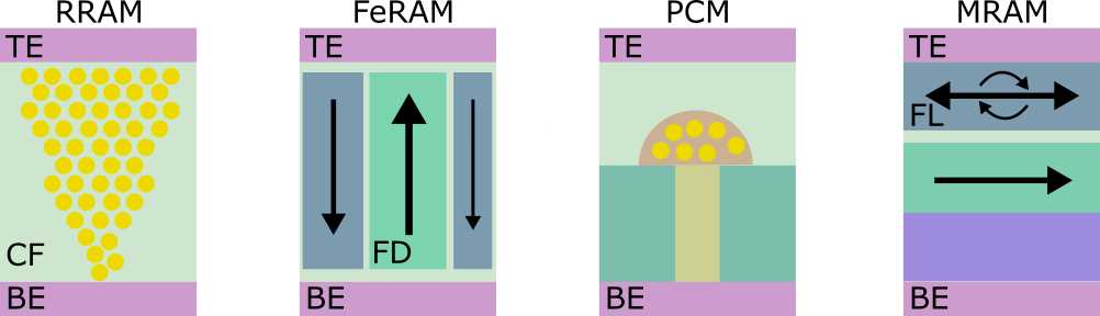
<p>If you’re here, you probably already know what memristors are, but in case you don’t: memristors are a novel class of electronic devices that exhibit interesting properties, including the ability to assume different resistance levels and hold their resistive state without requiring static power consumption. In a nutshell, they are non-volatile memories. Memristors can be made of different materials and, according to the physical principle they exploit, they are classified into the following main categories: Resistive-Random-Access-Memories (RRAMs) [1,2], Ferroelectric-RAMs (FeRAMs) [3,4], Phase-Change-Memories (PCMs) [5], and Magnetic-RAM (MRAM) [6].</p>

<p align="center">
<img src="/images/Blog_MAT/MAT_F1.png" width="750" />
<br />
<em>Different types of memristors: RRAMs feature a conductive resistive filament, FeRAMs multiple ferroelectric domains, PCM phase change materials, MRAMs magnetic domains.</em>
</p>

<h1 id="are-memristors-anygood">Are memristors any good?</h1>
<p>Yes, definitely! For the following reasons:</p>

<ul>
  <li>Small cell size → high integration density</li>
  <li>Multi-level states* → high memory density</li>
  <li>Non-volatility → (virtually) zero static power consumption</li>
</ul>

<p>*except for MRAMs, which are binary devices</p>

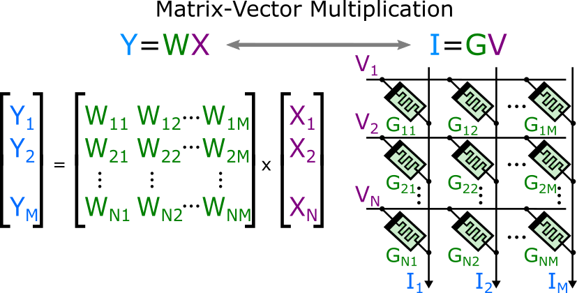
<p>In particular, memristors can be arranged in arrays and enable efficient in-memory matrix-vector multiplication (MVM). Weights from a matrix W can be mapped onto the conductances G in the memristive array, and the inputs X are presented as voltages V at the rows of the array. Exploiting Ohm’s and Kirchhoff’s laws, the currents at the columns, I, compute the MVM output Y = WX. If you know anything about neural networks, you’ll be aware that MVM operations are at the very core of neural-network computation. That’s where all the hype around memristive systems for artificial intelligence stems from.</p>

<p align="center">
<img src="/images/Blog_MAT/MAT_F2.png" width="750" />
<br />
<em>Efficient implementation of the Matrix-Vector-Multiplication (MVM) with a memristive array (right). Each weight in matrix W can be mapped to a conductance G in the memristive array.</em>
</p>

<h1 id="is-there-a-catch-with-memristors">Is there a catch with memristors?</h1>
<p>Well, yes, memristors also have their issues.</p>

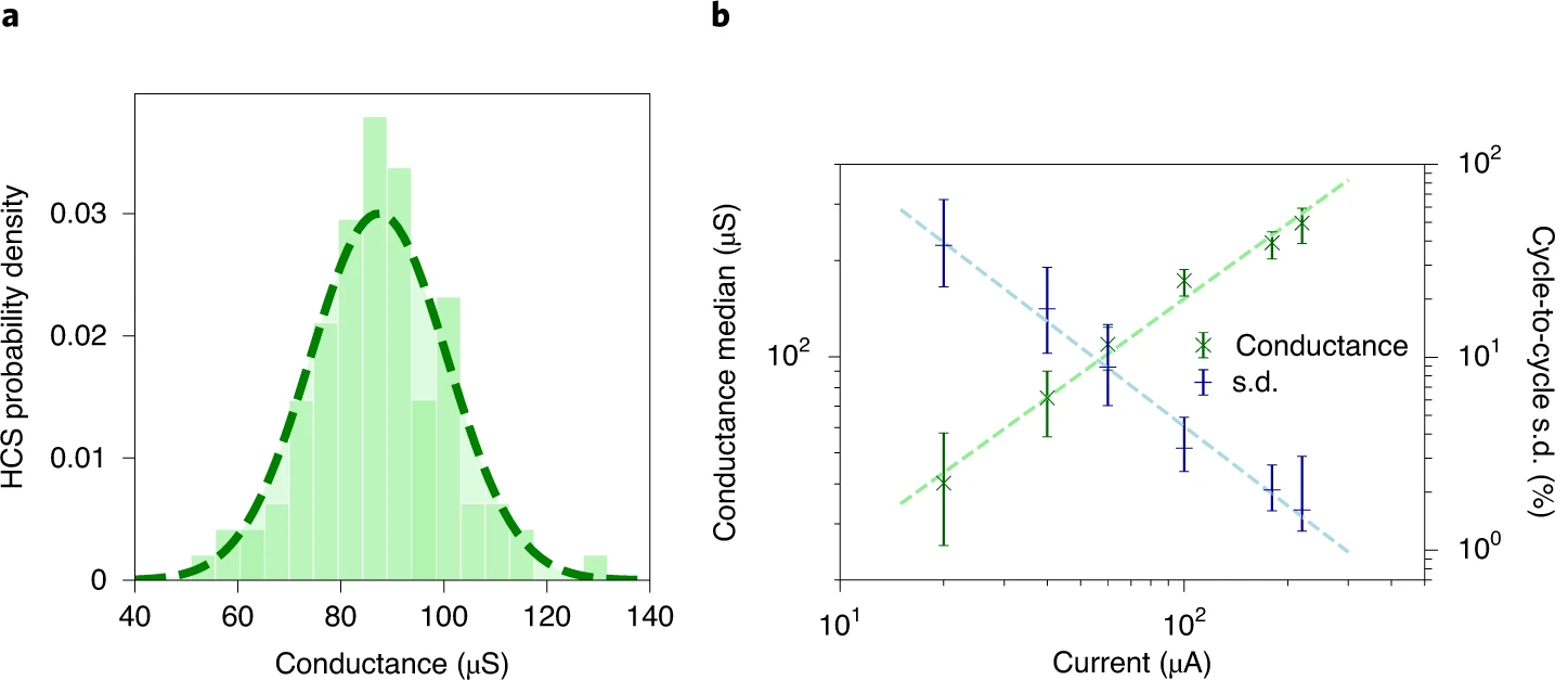
<p>The main issue with memristors is their <em>variability</em>. What does it mean? Imagine you have 100 memristors, you program them with the same programming conditions, and then you look at their state. You will observe a distribution of resistance levels due to so-called ‘<em>device-to-device</em>’ variability. Furthermore, if you program the same device 100 times, you will also observe a distribution of resistances due to ‘<em>cycle-to-cycle</em>’ variability. If you measure the state of a memristor over time, you might see its resistive level oscillate or even drift due to ‘<em>read-to-read</em>’ noise, ‘<em>random-telegraph-noise</em>’, and potentially even ‘<em>thermal-drift</em>’. Long story short, memristors suffer from variability and noise, which make it hard to precisely control their resistance. Although neural networks can tolerate slight imprecision in their weights, the amount of variability introduced by memristors generally disrupts neural-network performance.</p>

<p>Notice that the variability in RRAMs is in the [5–15]% interval, considering the mean resistance over the standard deviation. Other memristive technologies report similar levels of variability.</p>

<p align="center">
<img src="/images/Blog_MAT/MAT_F3.png" width="750" />
<br />
<em>Example of variability in RRAM devices. a) RRAM device-to-device variability after programming 4096 devices with the same programming conditions. HCS stands for High-Conductive-State. b) Measurement of cycle-to-cycle variability. The "Current" x-axis refers to the programming condition. From [7].</em>
</p>

<h1 id="is-there-a-fix-for-memristors-variability">Is there a fix for memristors’ variability?</h1>
<p>Yes, in the form of Memristive-Aware-Training! :)</p>

<p>The trick is to introduce device noise <strong>during training</strong>, so that the network gets used to memristor variability. Practically, such a training scheme aims to avoid narrow valleys in the loss function and find a flatter local minimum, where perturbations due to memristor variability create fewer problems. How can you introduce noise during training? With the Straight-Through-Estimator function. It’s a common technique for training quantized/binarized neural networks, and it consists of decoupling the weight matrices used for the forward and backward passes. In this way, one can use noisy memristive weights for inference and perform weight updates on the original unperturbed weights. To do this, all it takes is a simple function added to the forward pass of your neural network model. In PyTorch, this can be implemented as follows:</p>

<div class="language-plaintext highlighter-rouge"><div class="highlight"><pre class="highlight"><code># STE function to apply noise in the forward pass
class Noisy_Inference(torch.autograd.Function):
    """
    Function taking the weight tensor as input and applying gaussian noise with standard deviation 
    (noise_sd) and outputting the noisy version for the forward pass, but keeping track of the 
    original de-noised version of the weight for the backward pass
    """
    noise_sd = 1e-1

    @staticmethod
    def forward(ctx, input):
        """
        In the forward pass we add some noise from a gaussian distribution
        """
        ctx.save_for_backward( input )
        weight = input.clone()
        # registering the span of weight values
        delta_w = 2*torch.abs( weight ).max()
        # noise tensor to be applied to the weights
        noise = torch.randn_like( weight )*( Noisy_Inference.noise_sd * delta_w )
        return torch.add( weight, noise )

    @staticmethod
    def backward(ctx, grad_output):
        """
        In the backward pass we simply copy the gradient from upward in the computational graph
        """
        input, = ctx.saved_tensors
        weight = input.clone()
        return grad_output
noiser = Noisy_Inference.apply

# Application of the STE to a linear layer
# out_noisy = torch.nn.functional.linear( input, noiser(weight), noiser(bias) )
</code></pre></div></div>

<blockquote>
  <p><strong>Does Memristor-Aware-Training work?</strong> Yes, it does! Look at the results.</p>
</blockquote>

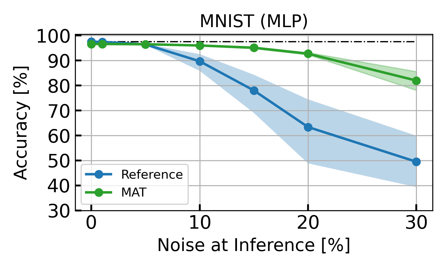
<p>As discussed, Memristor-Aware-Training (MAT) helps neural networks find a weight configuration that is resilient to perturbation. It’s very similar to the Quantization-Aware-Training technique [8], where model parameters are quantized during training to mitigate performance loss due to weight quantization for deployment on resource-constrained hardware (limited bit precision). In the same way, MAT makes the network resilient to memristor noise and variability. Check out the effect of MAT on the very common MNIST handwritten-digit recognition task under different weight-perturbation levels. In the example below, weights are perturbed both during training and during testing with Gaussian distributions whose standard deviation is normalized by the maximum weight magnitude (and reported as a percentage). The training noise standard deviation is 20%.</p>

<p align="center">
<img src="/images/Blog_MAT/MAT_F4.png" width="600" />
<br />
<em>Accuracy of a Multi-Layer Perceptron (size of 728–128–10) on MNIST under different weight perturbation magnitudes during Inference. Reference is trained without the noise injection, while MAT is trained with 20% noise injection.</em>
</p>

<p>So how does MAT work?</p>

<p>It’s really simple: all it takes is following these steps:</p>

<ul>
  <li>Pre-training without noise</li>
  <li>Activating the noise injection function on your model</li>
  <li>(Re-)Training with noise injection</li>
  <li>Deployment on memristive hardware :)</li>
</ul>

<p>This exact methodology has been adopted for very successful early implementations of Deep Neural Networks on memristive substrates, resulting in high-impact factor journal publications:</p>

<p>→ NeuRRAM [9]: an RRAM-based accelerator demonstrated with a ResNet-20 on CIFAR10, with &gt;88% accuracy on-chip.
→ Joshi, Vinay, et al. “Accurate deep neural network inference using computational phase-change memory.” Nature Communications 11.1 (2020): 2473. [10], where a ResNet-32 reaches 71.6% accuracy on ImageNet.</p>

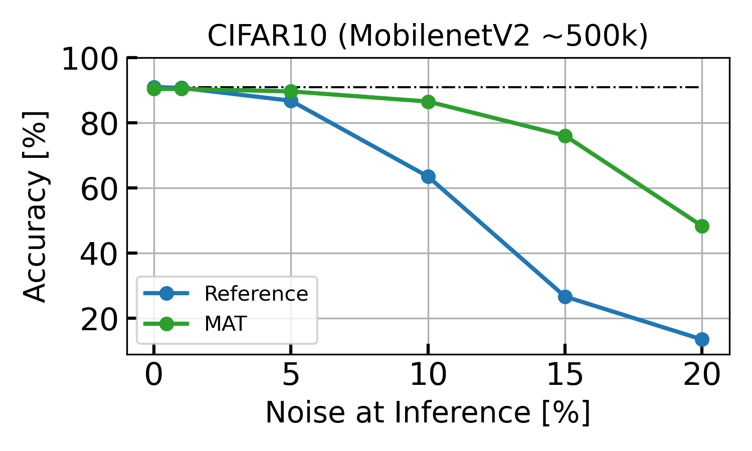
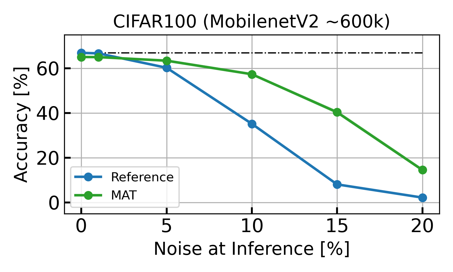
<p>With a similar methodology, MAT is demonstrated in simulation with a MobileNet-V2 network on the CIFAR-10/100 tasks, with the following results.</p>

<p align="center">
<img src="/images/Blog_MAT/MAT_F5.png" width="600" />
<br />
</p>

<p align="center">
<img src="/images/Blog_MAT/MAT_F6.png" width="600" />
<br />
</p>

<p>Notably, the technique described above is not the only one proven successful for deploying neural networks on memristive substrates. A solution is proposed in [11], accounting for memristive non-linearity in the training phase, while [12] introduces noise during training with Bayesian-optimized dropout layers. Possibly, these techniques could be complementary and might even be combined with Memristor-Aware-Training to yield better results.
This post aims to spread knowledge about the Memristor-Aware-Training technique and promote the development of memristive systems for artificial intelligence, which have strong potential to become a disruptive technology for edge-AI applications. For this reason, the code to obtain the results shown in this post is shared on the following GitHub page, belonging to the EIS group.</p>

<p>Visit the <a href="https://medium.com/r?url=https%3A%2F%2Fgithub.com%2FEIS-Hub%2FMemristor-Aware-Training.git">Memristor-Aware-Training GitHub repo</a>.</p>

<p>Also check out the Emerging Intelligent Substrates Lab (EIS), directed by Melika Payvand. It’s a cool environment where novel memristive-based architectures and neuromorphic algorithms are co-designed, leading to creative and competitive neuromorphic solutions.</p>

<p>Visit the <a href="https://github.com/EIS-Hub">EIS Lab GitHub</a>.</p>

<h1 id="references">References</h1>
<p>[1] Wong, H-S. Philip, et al. “Metal–oxide RRAM.” Proceedings of the IEEE 100.6 (2012): 1951–1970.</p>

<p>[2] Kim, M. J., et al. “Low power operating bipolar TMO ReRAM for sub 10 nm era.” 2010 International Electron Devices Meeting. IEEE, 2010.</p>

<p>[3] Mikolajick, Thomas, et al. “FeRAM technology for high density applications.” Microelectronics Reliability 41.7 (2001): 947–950.</p>

<p>[4] L. Grenouillet et al. “Performance assessment of BEOL-integrated HfO 2-based ferroelectric capacitors for FeRAM memory arrays”. In: 2020 IEEE Silicon Nanoelectronics Workshop (SNW). IEEE. 2020, pp. 5–6.</p>

<p>[5] Ielmini, Daniele, et al. “Physical interpretation, modeling and impact on phase change memory (PCM) reliability of resistance drift due to chalcogenide structural relaxation.” 2007 IEEE International Electron Devices Meeting. IEEE, 2007.</p>

<p>[6] Na, Taehui, Seung H. Kang, and Seong-Ook Jung. “STT-MRAM sensing: a review.” IEEE Transactions on Circuits and Systems II: Express Briefs 68.1 (2020): 12–18.</p>

<p>[7] Dalgaty, Thomas, et al. “In situ learning using intrinsic memristor variability via Markov chain Monte Carlo sampling.” Nature Electronics 4.2 (2021): 151–161.</p>

<p>[8] Jacob, Benoit, et al. “Quantization and training of neural networks for efficient integer-arithmetic-only inference.” Proceedings of the IEEE conference on computer vision and pattern recognition. 2018.</p>

<p>[9] Wan, Weier, et al. “A compute-in-memory chip based on resistive random-access memory.” Nature 608.7923 (2022): 504–512.</p>

<p>[10] Joshi, Vinay, et al. “Accurate deep neural network inference using computational phase-change memory.” Nature Communications 11.1 (2020): 2473.</p>

<p>[11] Joksas, Dovydas, et al. “Nonideality‐Aware Training for Accurate and Robust Low‐Power Memristive Neural Networks.” Advanced Science 9.17 (2022): 2105784.</p>

<p>[12] Ye, Nanyang, et al. “Improving the robustness of analog deep neural networks through a Bayes-optimized noise injection approach.” Communications Engineering 2.1 (2023): 25.</p>]]></content><author><name>Filippo Moro</name><email>filippo.moro@uzh.ch</email></author><category term="Memristors" /><category term="Machine Learning" /><category term="Edge AI" /><summary type="html"><![CDATA[Memristors: a controversial technology with as many supporters as critics. Memristors have attracted considerable attention in the edge-AI industry as a promising memory technology capable of improving energy efficiency and integration density by orders of magnitude compared with standard integrated memory. However, the memristive revolution has been hindered (or delayed) by many technical difficulties. Among these is the problem of variability, i.e., the stochastic behavior memristors exhibit in their conductance during programming. Is it a dealbreaker? This article shows how to address memristive-conductance variability with a particular training methodology inspired by Quantization-Aware-Training, a method used to train heavily quantized networks. The so-called Memristor-Aware-Training introduces memristor-calibrated variability during training so that optimization can adapt to it and converge to a stable weight configuration that tolerates variability.]]></summary></entry></feed>